 |
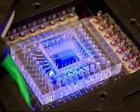
Berkeley CA (SPX) Feb 07, 2011 Engineers at the University of California, Berkeley, have found a way to grow nanolasers directly onto a silicon surface, an achievement that could lead to a new class of faster, more efficient microprocessors, as well as to powerful biochemical sensors that use optoelectronic chips. They describe their work in a paper to be published Feb. 6 in an advanced online issue of the journal Nature Photonics. "Our results impact a broad spectrum of scientific fields, including materials science, transistor technology, laser science, optoelectronics and optical physics," said the study's principal investigator, Connie Chang-Hasnain, UC Berkeley professor of electrical engineering and computer sciences. The increasing performance demands of electronics have sent researchers in search of better ways to harness the inherent ability of light particles to carry far more data than electrical signals can. Optical interconnects are seen as a solution to overcoming the communications bottleneck within and between computer chips. Because silicon, the material that forms the foundation of modern electronics, is extremely deficient at generating light, engineers have turned to another class of materials known as III-V (pronounced "three-five") semiconductors to create light-based components such as light-emitting diodes (LEDs) and lasers. But the researchers pointed out that marrying III-V with silicon to create a single optoelectronic chip has been problematic. For one, the atomic structures of the two materials are mismatched. "Growing III-V semiconductor films on silicon is like forcing two incongruent puzzle pieces together," said study lead author Roger Chen, a UC Berkeley graduate student in electrical engineering and computer sciences. "It can be done, but the material gets damaged in the process." Moreover, the manufacturing industry is set up for the production of silicon-based materials, so for practical reasons, the goal has been to integrate the fabrication of III-V devices into the existing infrastructure, the researchers said. "Today's massive silicon electronics infrastructure is extremely difficult to change for both economic and technological reasons, so compatibility with silicon fabrication is critical," said Chang-Hasnain. "One problem is that growth of III-V semiconductors has traditionally involved high temperatures - 700 degrees Celsius or more - that would destroy the electronics. Meanwhile, other integration approaches have not been scalable." The UC Berkeley researchers overcame this limitation by finding a way to grow nanopillars made of indium gallium arsenide, a III-V material, onto a silicon surface at the relatively cool temperature of 400 degrees Celsius. "Working at nanoscale levels has enabled us to grow high quality III-V materials at low temperatures such that silicon electronics can retain their functionality," said Chen. The researchers used metal-organic chemical vapor deposition to grow the nanopillars on the silicon. "This technique is potentially mass manufacturable, since such a system is already used commercially to make thin film solar cells and light emitting diodes," said Chang-Hasnain. Once the nanopillar was made, the researchers showed that it could generate near infrared laser light - a wavelength of about 950 nanometers - at room temperature. The hexagonal geometry dictated by the crystal structure of the nanopillars creates a new, efficient, light-trapping optical cavity. Light circulates up and down the structure in a helical fashion and amplifies via this optical feedback mechanism. The unique approach of growing nanolasers directly onto silicon could lead to highly efficient silicon photonics, the researchers said. They noted that the miniscule dimensions of the nanopillars - smaller than one wavelength on each side, in some cases - make it possible to pack them into small spaces with the added benefit of consuming very little energy "Ultimately, this technique may provide a powerful and new avenue for engineering on-chip nanophotonic devices such as lasers, photodetectors, modulators and solar cells," said Chen. "This is the first bottom-up integration of III-V nanolasers onto silicon chips using a growth process compatible with the CMOS (complementary metal oxide semiconductor) technology now used to make integrated circuits," said Chang-Hasnain. "This research has the potential to catalyze an optoelectronics revolution in computing, communications, displays and optical signal processing. In the future, we expect to improve the characteristics of these lasers and ultimately control them electronically for a powerful marriage between photonic and electronic devices."
Share This Article With Planet Earth
Related Links University of California, Berkeley Computer Chip Architecture, Technology and Manufacture Nano Technology News From SpaceMart.com
 Silicon Oxide Gets Into The Electronics Action On Computer Chips
Washington DC (SPX) Jan 21, 2011 In the materials science equivalent of a football fan jumping onto the field and scoring a touchdown, scientists are documenting that one fundamental component of computer chips, long regarded as a passive bystander, can actually be made to act like a switch. That potentially allows it to take part in the electronic processes that power cell phones, iPads, computers, and thousands of other ... read more |
|
| The content herein, unless otherwise known to be public domain, are Copyright 1995-2010 - SpaceDaily. AFP and UPI Wire Stories are copyright Agence France-Presse and United Press International. ESA Portal Reports are copyright European Space Agency. All NASA sourced material is public domain. Additional copyrights may apply in whole or part to other bona fide parties. Advertising does not imply endorsement,agreement or approval of any opinions, statements or information provided by SpaceDaily on any Web page published or hosted by SpaceDaily. Privacy Statement |


 del.icio.us
 Digg
Digg Reddit
 YahooMyWeb
 Google