|
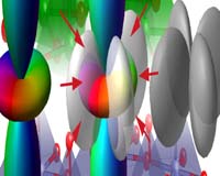
Fayetteville AR (SPX) Oct 16, 2007 A University of Arkansas researcher and his colleagues have found a novel way to "look" at atomic orbitals, and have directly shown for the first time that they change substantially when interacting at the interface of a ferromagnet and a high-temperature superconductor. This finding opens up a new way of designing nanoscale superconducting materials and fundamentally changes scientific convention, which suggests that only electron spin and atomic charge - not atomic orbitals - influence the properties of superconducting nanostructures. It also has implications for interfaces between other complex oxide materials. Jacques Chakhalian, assistant professor of physics in the J. William Fulbright College of Arts and Sciences, and his colleagues will publish their findings online at Science Express. Until now, materials science researchers believed that an electron's charge and spin influenced the characteristics of conventional bulk materials. Atomic orbitals, which consist of the patterns of electron density that may be formed in an atom, were previously thought to be inactive. "In conventional materials like copper or silicon, you could account for everything you could see through charge and spin," Chakhalian said. Further, orbitals have proved difficult to "see" through physical experimentation, so it wasn't possible to examine any changes in orbital symmetry that might be taking place at the interface. Chakhalian's work has focused on what happens at the interface between two different materials - for instance, superconductors and ferromagnets, two materials with properties that were thought to be incompatible with each other in bulk. In 2006, he and his colleagues created the first high-quality material to have both superconducting and ferromagnetic properties, and they used that material in this experiment. Chakhalian and his colleagues worked with synchrotron radiation at the Advanced Photon Source, Argonne National Laboratory in Argonne, Ill., to examine the interface between a high-temperature superconducting material containing copper oxide and a ferromagnetic material containing manganese oxide. The synchrotron light is electromagnetic radiation of varying wavelengths that can be tuned to a specific wavelength and polarization for a particular experiment. Unlike conventional X-rays, which diffuse through space, the synchrotron light beams are sharply focused, like a laser beam with extreme brilliance. The researchers forced the two materials into unusual quantum states. Using a technique called resonant X-ray absorption, they were able to "look" at the atomic orbitals at the interface and determine their symmetry in a non-destructive way. They found that the atomic orbitals changed the nature of their symmetry at the interface and created a covalent bond between the copper and manganese atoms. This bonding does not exist in the bulk of the individual materials "When you merge these two materials, the atomic orbitals at the interface become important. They start contributing to the electronic properties of the material," Chakhalian said. "This opens a new way of designing materials. We can design quantum materials with engineered physical properties." The discovery may allow researchers to manipulate nanoscale superconductivity at the interface - opening the possibility of creating room-temperature semiconductors. Generators that use superconducting materials generate electricity extremely efficiently, at half the size of conventional generators. General Electric estimates the potential market for superconducting generators to be between $20 billion and $30 billion over the next decade. Chakhalian's colleagues include J.W. Freeland and M. van Veenendaal of the Advanced Photon Source, Argonne National Laboratory, Argonne, Ill.; and H.-U. Habermeier, G. Cristiani, G. Khaliullin and B. Keimer of the Max Planck Institute for Solid State Research in Stuttgart, Germany. Related Links University of Arkansas, Fayetteville Nano Technology News From SpaceMart.com Computer Chip Architecture, Technology and Manufacture
 Washington DC (SPX) Oct 12, 2007
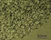
Some nanotechnology fanciers suggest that, like proverbial birds of a feather, engineered nanoscale materials will flock - or clump - together. This tendency, they maintain, should reduce or eliminate risks as nanotechnology manufacturing increases and the number of nanotechnology-enabled products grows. |
|
| The content herein, unless otherwise known to be public domain, are Copyright Space.TV Corporation. AFP and UPI Wire Stories are copyright Agence France-Presse and United Press International. ESA Portal Reports are copyright European Space Agency. All NASA sourced material is public domain. Additional copyrights may apply in whole or part to other bona fide parties. Advertising does not imply endorsement, agreement or approval of any opinions, statements or information provided by Space.TV Corp on any Web page published or hosted by Space.TV Corp. Privacy Statement |