 |
Santa Barbara CA (SPX) May 23, 2011 Researchers at Hewlett Packard and the University of California, Santa Barbara, have analysed in unprecedented detail the physical and chemical properties of an electronic device that computer engineers hope will transform computing. Memristors, short for memory resistors, are a newly understood circuit element for the development of electronics and have inspired experts to seek ways of mimicking the behaviour of our own brains' activity inside a computer. Research in IOP Publishing's Nanotechnology, explains how the researchers have used highly focused x-rays to map out the nanoscale physical and chemical properties of these electronic devices. It is thought memristors, with the ability to 'remember' the total electronic charge that passes through them, will be of greatest benefit when they can act like synapses within electronic circuits, mimicking the complex network of neurons present in the brain, enabling our own ability to perceive, think and remember. Mimicking biological synapses - the junctions between two neurons where information is transmitted in our brains - could lead to a wide range of novel applications, including semi-autonomous robots, if complex networks of neurons can be reproduced in an artificial system. In order for the huge potential of memristors to be utilised, researchers first need to understand the physical processes that occur within the memristors at a very small scale. Memristors have a very simple structure - often just a thin film made of titanium dioxide between two metal electrodes - and have been extensively studied in terms of their electrical properties. For the first time, researchers have been able to non-destructively study the physical properties of memristors allowing for a more detailed insight into the chemistry and structure changes that occur when the device is operating. The researchers were able to study the exact channel where the resistance switching of memristors occurs by using a combination of techniques. They used highly focused x-rays to locate and image the approximately one hundred nanometer wide channel where the switching of resistance takes place, which could then be fed into a mathematical model of how the memristor heats up. John Paul Strachan of the nanoElectronics Research Group, Hewlett-Packard Labs, California, said: "One of the biggest hurdles in using these devices is understanding how they work: the microscopic picture for how they undergo such tremendous and reversible change in resistance. "We now have a direct picture for the thermal profile that is highly localized around this channel during electrical operation, and is likely to play a large role in accelerating the physics driving the memristive behavior." This research appears as part of a special issue on non-volatile memory based on nanostructures. "The switching location of a bipolar memristor: Chemical, thermal, and structural mapping" (Nanotechnology, 22 254015) will be freely available online from Monday, 16 May.
Share This Article With Planet Earth
Related Links Institute of Physics Nano Technology News From SpaceMart.com Computer Chip Architecture, Technology and Manufacture
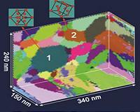 Looking inside nanomaterials in three dimensions
Frederiksborgvej, Denmark (SPX) May 19, 2011 The journal Science has published a paper where scientists from Riso DTU in collaboration with scientists from China and USA, have reported a new method for revealing a 3D picture of the structure inside a material. Most solid materials are composed of millions of small crystals, packed together to form a fully dense solid. The orientations, shapes, sizes and relative arrangement of these ... read more |
|
| The content herein, unless otherwise known to be public domain, are Copyright 1995-2010 - SpaceDaily. AFP and UPI Wire Stories are copyright Agence France-Presse and United Press International. ESA Portal Reports are copyright European Space Agency. All NASA sourced material is public domain. Additional copyrights may apply in whole or part to other bona fide parties. Advertising does not imply endorsement,agreement or approval of any opinions, statements or information provided by SpaceDaily on any Web page published or hosted by SpaceDaily. Privacy Statement |


 del.icio.us
 Digg
Digg Reddit
 YahooMyWeb
 Google